Designed by SM6MUY, Bengt and SM6PGP, Hannes
VCXO with PLL to be locked to any kind of frequeny reference. The first version was built approx 1995. Now several modification have been done. The latest was to remove the eeprom and some HC-logic and to replace it with a PIC 16C84/16F84 that can be programmed on board.
The heart of the design is an emitter coupled harmonic oscillator( BFS520) which have good short term stability. (RF design, Oscillator design handbook) It is easy to add a varactor in this circuit to pull the oscillator an small amount in frequency. The oscillator is followed by a transistor buffer (BFS520). The signal is fed into an attenuator and a small Si MMIC (MSA2111) to further increase isolation towards the oscillator. In some cases I have used the MMIC as a multipler. Then the attenuator is adjusted to make the MMIC go into compression it is followed by a helixfilter(TOKO) to select the wanted harmonic. The resistor in the bias circuit can be optimized to improve conversion loss in the multiplier.
The synthesizer is a Siemens/Infineon PMB2306T wich is loaded with
serial
data, Data-Enable-Clock. The signals for loading the synt is generated
by the PIC processor 16C84/16F84. The PIC can be programmed on board
just
by removing two 0ohm jumpers. I use MPLAB from Microchip and a
programmer
attached to the PC parallell port. I will add some examples of code for
the PIC processor on this page later.
Programming software: look for PICPROG by Conquest systems (ZL1HIT)
a very nice pice of software and a good description of the needed
hardwar, or IC-PROG (added 2004-10-26)..
Some possible combinations of oscillator and reference frequencies:
OSC FQ REF FQ N-div R-div(13 MHz) R-div(10 MHz) R-div(5MHz)
90.666666 MHz 333.333
kHz
272
39
30
15
(2320 MHz xverter)
96.000000 MHz 500
kHz
192
26
20
10
(1296 MHz xverter)
106.50000 MHz 500
kHz
213
26
20
10
(10368 MHz xverter)
108.06666 MHz 66.6666 kHz
1621
195
150
75 (SK6MHI 1296.800 MHz)
117.00000 MHz 500
kHz
234
26
20
10
(5760 MHz xverter)
125.50000 MHz 500
kHz
251
26
20
10
(24192 MHz xverter)
128.00000 MHz 500
kHz
256
26
20
10
(1296 MHz xverter)
The PLL loop filter has to be designed for the selected reference
frequency.
There is no component values in the component placing drawing.
Use PLL loop filter design by National Semiconductor. I have
used a 3:rd order filter. Kvco has to be measured (typical 1-2 kHz/V).
Loop BW has to be selected (10 -100 Hz gives reasonable component
values)
An example of a loopfilter :
fosc = 90.666666
MHz
C1 = 33nF
fref = 333.333333
kHz
C2 = 330 nF
Ndiv =
272
R2 = 56 k
Rdiv = 15 (5 MHz reference
osc)
R3 = 120 k
Kvco = 1
kHz/V
C3 = 120 pF
Icp = 1 mA
Att = 60 dB
Phase marg = 56 deg
loop BW = 30 Hz
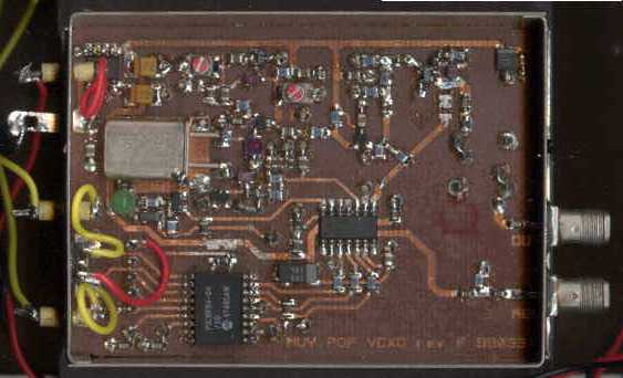
The VCXO/PLL can be built in a standard 55 x 72 mm tinplate
box
NEW
2004-10-26
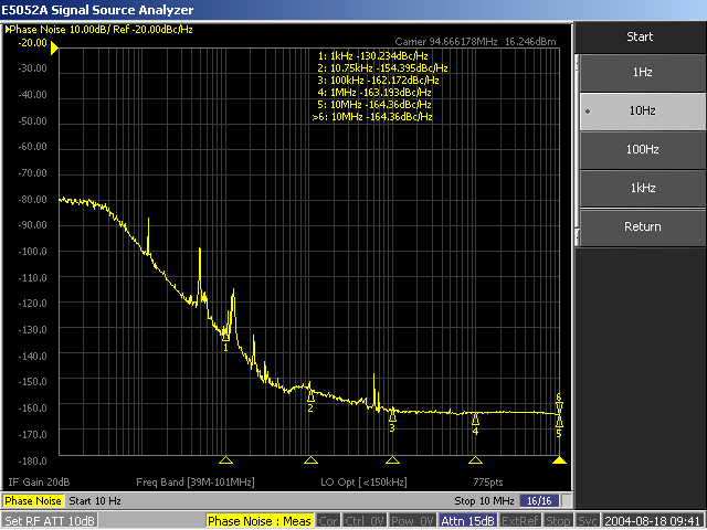
VCXO Phase noise measurement
A phase noise measurment has been performed with the new
AGILENT E5052 Signal Source Analyzer. I got this
opportunity at an Agilent instrument demonstration.
Thanks to the Agilent guys !
Things, good to know if you are trying to build this VCXO.
The xtall has to be approx 3 - 4 kHz higher in frequency than the
wanted
fq. So if you plan building it for 106.5 MHz then you have to order an
xtall for 106.503 MHz, this is because the wanted pulling range is +/-
3 kHz. I do usually order 5:th overtone series resonant xtalls.
Run the oscillator and connect a trimpot to gnd and +5 V) and the wiper
to the cap-diode so you can check that the osc is running ok and that
you
get the wanted pulling range. Tune the trimcaps in the osc so that you
get approx 2.5 V when you are at the centerfq and so that the
oscillator
starts at power on. The inductor and the type of capdiode affect the
pulling
range, you may have to change these. The inductor usually ends up in
the
range 100-390 nH.
In some cases it has been necessary to remove the 2.2 pF cap mounted from base of the osc transistor to ground.
Change from rev F to rev G, I found that there was a capacitor (1 nF) lost at the bias of MSA2111 between the inductor and the resistor. Should be connected from the connecting point of the 39 ohm/220nH and to gnd.
Unfortunately I have found out that the
PMB2306
is becomming obsolete !
I have no plans in modifying the vcxo circuit
to accomodate a new synthezeiser. 2001-04-13
Schematic in pdf or in postscript format:
schematic in pdf (35k)
schematic in encapsulated postscript
(64k)
PCB layout in pdf or in postscript format:
Board layout in pdf (30k)
Board layout in encapsulated postscript
(124k)
Component placement in pdf or in postscript format:
Component placement in pdf (21k)
Component placement in encapsulated
postscript (38k)
Use GSview to view postscript documents or download and print on a postscript printer.
NEW 2001-04-13
PIC asm and hex code examples (16C84), the code is as it is and i
have
not put much effort in the programming
as I am no programmer and just do it because I have to.
Anyone who likes to create better code may do so and I am interested
in a copy.
106.5 MHz (LO for 10 GHz xverter)
ref = 500 kHz
vcxo1065.asm
vcxo1065.hex
125.111111.... MHz (LO for P3D 23/13 cm up/dwn link)
ref = 111.111 111...kHz
vcxo1251.asm
vcxo1251.hex
Info for creating the databytes
in
the asm-code
Refer to datasheet for the PMB2306
Information on
this page may only be used for personal use, for any other use pse contact (s m
6 p g p ( a t ) i l l i p e . s e)
Changed 2014-07-26 by SM6PGP